SFA-AM - Strategic Focus Area Advanced Manufacturing
  • Home
  • Focus Areas
    • Focus Areas 2017-2020 >
      • Precision Free-Form Manufacturing
      • Printed Electronics
      • Sustainable Digital Manufacturing and Design
      • Sensing Technologies
      • Intelligent Systems and Advanced Automation
    • Focus Areas 2021-2024 >
      • Manufacturing Technologies
      • Functionality Integration
      • Sensing Technologies
      • Intelligent Systems and Advanced Automation
  • Projects
    • Projects Initial Program 2017-2020 >
      • Ceramic X.0
      • FUORCLAM
      • Powder Focusing
      • PREAMPA
      • FOXIP
      • CFRP-AM
      • SD4D
    • Projects Expansion Program 2017-2020 >
      • D-SENSE
      • MOCONT
      • Nano Assembly
      • SOL4BAT
    • Projects Program 2021-2024 >
      • AMYS
      • ClosedLoop-LM
      • DiPrintProtect
      • MANUFHAPTICS
      • Microfluidics
      • Multi-Mat
      • SCALAR
      • SMARTAM
  • Events
    • Annual Meetings >
      • Annual Review Meeting 2022
      • Annual Review Meeting 2021
      • Annual Review Meeting 2020
      • Annual Review Meeting 2019
      • Annual Review Meeting 2018
    • Industry Workshops >
      • Sensors
    • Other Events >
      • CERAMIC X.0 Workshop
      • Workshop 13 July 2020
      • Launch Event 13 Nov 2017
      • Workshop 6 July 2017
      • Workshop 17 Oct 2016
    • SAMCE
  • About
    • Steering Committee
    • Participating ETH Institutions
    • Calls & Selection >
      • Initial Program 2017-2020
      • Expansion Program 2017-2020
      • Continuation Program 2021-2024
  • Contact

AMYS

Advancing Manufacturability of Hybrid Organic-inorganic Semiconductors for Large Area Optoelectronics
Background and main goal
Optoelectronic technologies based on a perovskite semiconductor promise numerous advantages over existing options: a lower levelized cost of solar electricity, colour-pure light-emitting diode displays, and highly sensitive detectors for photons, X-rays, or gamma rays. The challenge is that best-performing perovskite materials still degrade too rapidly to make any of these applications economically viable at this stage of research. Furthermore, performance quickly decreases when increasing the size of devices towards industry-relevant dimensions.

AMYS aims to overcome these limitations by (i) exploring the compositional space of perovskites to find compositions most suited for upscaling, (ii) understanding of how processing conditions can be modulated to improve optoelectronic properties and stability of the resulting thin films, and (iii) advancing the manufacturability of perovskites by demonstrating large-area optoelectronic devices that exhibit high performance and stability.

Idea and approach
Picture
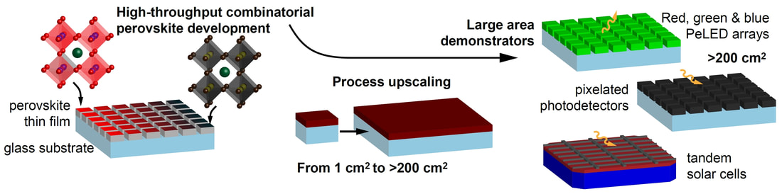
The AMYS project is centred on the identification of novel perovskite thin-film formulations and their deposition on large areas with novel industry-compatible processes. More specifically, AMYS will:
  • Identify most promising hybrid organic-inorganic metal halide thin film compositions and corresponding processing parameters using a high-throughput combinatorial approach,
  • select defect tolerant combinations of precursors and processing parameters that are most suited for upscaling,
  • design manufacturing methods to deposit the most promising perovskite thin films on large flexible substrates or highly textured substrates, and
  • validate the new compositions and thin-film deposition methods by demonstrating efficient and stable devices featuring large dimensions (larger than 200 cm^2).

To accomplish its objectives, the AMYS project will be organised around two 'pipelines' to bring compositions and processing conditions from small thin films to large-area functional devices of industrial relevance:
  • Pipeline 1: Known perovskite compositions and their deposition over large areas on flexible or textured substrates using innovative processes.
  • Pipeline 2: New compositions, from their discovery at high throughput using a combinatorial approach, their validation in small devices up until their incorporation in large-area devices.
Demonstrators
Picture
Picture
  • Large-area perovskite/silicon tandem solar cells on textured silicon wafers
  • Flexible pixelated photodetector arrays
  • Micropatterned monochromatic RGB perovskite light-emitting diode (PeLED) arrays
Technical challenges
  • Exploration of the rich compositional space of perovskites to identify formulations and processing conditions that result in thin films with suitable optoelectronic properties and operational stability for different applications
  • Development of deposition methods and corresponding process parameters to upscale perovskite thin films on various types of flexible and/or textured substrates to industry-relevant dimensions (>200 cm^2), while maintaining performance and operational stability
Consortium
Picture
Photovoltaics and Thin Film Electronics Laboratory, ​
​
EPF Lausanne

Prof. Dr. Christophe Ballif (project leader)
Dr. Christian Wolff
Quentin Jean-Marie Armand Guesnay (PhD student)
Picture
Thin Films and Photovoltaics Laboratory, ​
Empa
Prof. Dr. Ayodhya Tiwari (principal investigator)
Dr. Fan Fu
Radha Kothandaraman (PhD student)
Picture
Nanomaterials Engineering Research Group,
​ETH Zürich
Prof. Dr. Chih-Jen Shih (principal investigator)
Gerrit Stemmler (PhD student)
Picture
Laboratory for Surface Science and Coating Technologies​, ​
Empa
Dr. Sebastian Siol (principal investigator)
Alexander Wieczorek (PhD student)
Involved and supporting industry partners
  • Avantama AG
  • Flisom AG
  • Fluxim AG
  • Meyer Burger Research AG
Key project data 
Project Duration:
June 2021 – May 2025 (48 months)
Project Funding:
1.55 million CHF
Linked scientific publications
  • Kothandaraman, R. K., H. Lai, A. Aribia, S. Nishiwaki, S. Siegrist, M. Krause, Y. Zwirner, G. T. Sevilla, K. Artuk, C. M. Wolff, R. Carron, A. N. Tiwari and F. Fu (2022). "Laser Patterned Flexible 4T Perovskite-Cu(In,Ga)Se2 Tandem Mini-module with Over 18% Efficiency." Solar RRL 6(9): 2200392.
  • Lai, H., J. Luo, Y. Zwirner, S. Olthof, A. Wieczorek, F. Ye, Q. Jeangros, X. Yin, F. Akhundova, T. Ma, R. He, R. K. Kothandaraman, X. Chin, E. Gilshtein, A. Müller, C. Wang, J. Thiesbrummel, S. Siol, J. M. Prieto, T. Unold, M. Stolterfoht, C. Chen, A. N. Tiwari, D. Zhao and F. Fu (2022). "High-Performance Flexible All-Perovskite Tandem Solar Cells with Reduced VOC-Deficit in Wide-Bandgap Subcell." Advanced Energy Materials 12(45): 2202438.
  • Wieczorek, A., H. Lai, J. Pious, F. Fu and S. Siol "Resolving Oxidation States and X–site Composition of Sn Perovskites through Auger Parameter Analysis in XPS." Advanced Materials Interfaces n/a(n/a): 2201828.
An initiative of the ETH Board
Picture
Participating Institutions of the ETH Domain
Picture
Picture
Picture
Picture
Disclaimer
Imprint
© COPYRIGHT 2021. ALL RIGHTS RESERVED.
  • Home
  • Focus Areas
    • Focus Areas 2017-2020 >
      • Precision Free-Form Manufacturing
      • Printed Electronics
      • Sustainable Digital Manufacturing and Design
      • Sensing Technologies
      • Intelligent Systems and Advanced Automation
    • Focus Areas 2021-2024 >
      • Manufacturing Technologies
      • Functionality Integration
      • Sensing Technologies
      • Intelligent Systems and Advanced Automation
  • Projects
    • Projects Initial Program 2017-2020 >
      • Ceramic X.0
      • FUORCLAM
      • Powder Focusing
      • PREAMPA
      • FOXIP
      • CFRP-AM
      • SD4D
    • Projects Expansion Program 2017-2020 >
      • D-SENSE
      • MOCONT
      • Nano Assembly
      • SOL4BAT
    • Projects Program 2021-2024 >
      • AMYS
      • ClosedLoop-LM
      • DiPrintProtect
      • MANUFHAPTICS
      • Microfluidics
      • Multi-Mat
      • SCALAR
      • SMARTAM
  • Events
    • Annual Meetings >
      • Annual Review Meeting 2022
      • Annual Review Meeting 2021
      • Annual Review Meeting 2020
      • Annual Review Meeting 2019
      • Annual Review Meeting 2018
    • Industry Workshops >
      • Sensors
    • Other Events >
      • CERAMIC X.0 Workshop
      • Workshop 13 July 2020
      • Launch Event 13 Nov 2017
      • Workshop 6 July 2017
      • Workshop 17 Oct 2016
    • SAMCE
  • About
    • Steering Committee
    • Participating ETH Institutions
    • Calls & Selection >
      • Initial Program 2017-2020
      • Expansion Program 2017-2020
      • Continuation Program 2021-2024
  • Contact