Nano AssemblyAutomated process flow for high-speed additive nanostructure assembly with integrated process control
Chiral: The nano factory
As an ETH spin-off rooted in the Nano Assembly project, Chiral is currently industrializing the results. We aim to serve customers with our unprecedented fabrication capability for nanocarbon devices. Together, we will unlock a new generation of applications such as quantum technology, IoT sensors, and more. Please watch our video, showing our wafer-level production chain in action. If you are interested please contact us at [email protected] or visit our website www.chiralnano.com.
Project
Background and Main Goal
Ultra-low power sensors are key components in mobile and autonomous systems, for the Internet of Things, and as functional elements in wearable systems for the Internet of Humans. Nanomaterials such as 1D nanotubes & nanowires and 2D materials have shown unique properties for ultra-sensitive, ultra-low power sensor applications. Single Walled Carbon Nanotubes (SWNT) devices have been successfully demonstrated for chemical and physical sensing at unprecedented low power consumption in the range of μW per sensor function.
Today, the biggest barrier for technology transfer or commercialization of SWNT or other nanomaterial sensors is the lack of an industrial manufacturing process for high device yield at low costs. The project aims to develop a new manufacturing process for nano electronic sensor systems, with functional nanostructures, demonstrated for Single Walled Carbon Nanotubes (SWNTs), but applicable beyond SWNTs. It includes aspects of machine learning, digitalization and requires adapted device design to exploit full functionality. The goal is to increase today’s state-of-the-art speeds by a factor of 1000 and to demonstrate that a fabrication of 1’000 components per hour is feasible.
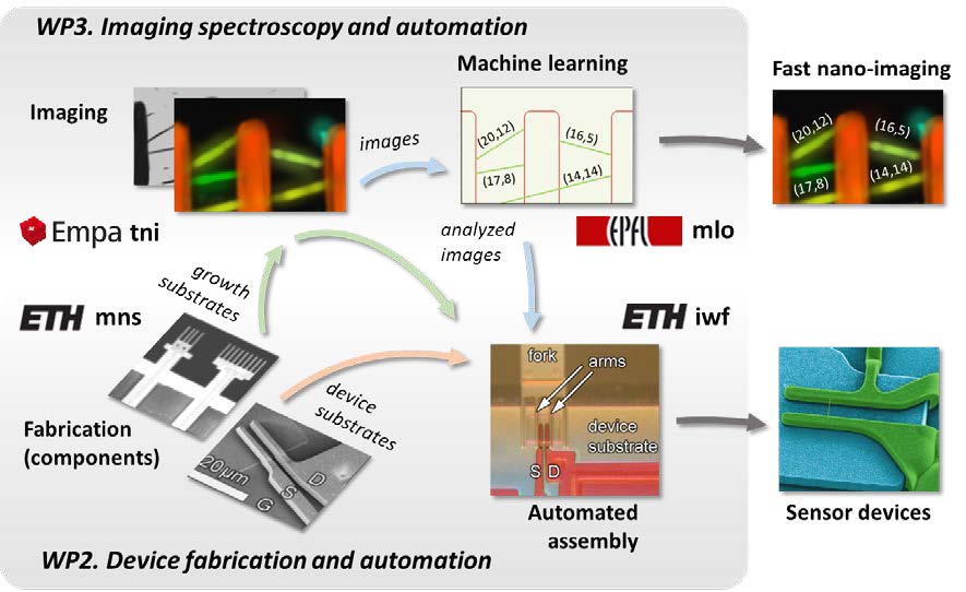
Structure of the Nano-Assembly project with two key work packages (WP)
Scope of Research Activities
➜ Develop an integrated process and system for the assembly of suspended SWNTs in devices ➜ Develop machine learning algorithms for process automation, control, and self-optimization ➜ Evaluate and implement high speed optical characterization processes for SWNTs Key Challenges and Technical Problems to Solve
➜ SWNT growth and integration of metallization ➜ Passivation of suspended SWNTs ➜ Speed of the optical characterization of SWNTs ➜ Accuracy of the mechanical assembly of nanostructures ➜ Machine learning methods to optimize data analysis Achievements and demonstrators
Batch growth of suspended carbon nanotubes
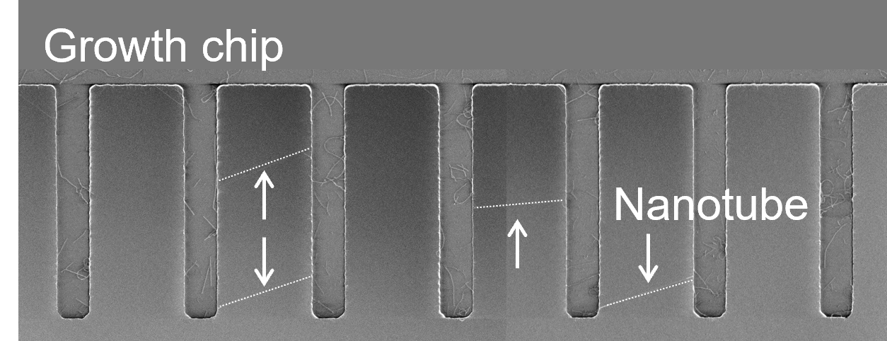
In a high-volume fabrication process for nanoelectronic devices, batch growth of high-quality nanostructures is the crucial first step. We have demonstrated the growth of 1000+ individual, suspended carbon nanotubes on a single growth substrate. This is a 50-fold improvement compared to previous work in the literature. A large-scale growth substrate, which hosts ~6000 cantilever pairs has been developed. In parallel, multi-component parameter optimization has been performed to optimize the density of cantilever pairs with exactly one suspended carbon nanotube. Contact: Dr. Cosmin Roman Involved research groups: ETH Zurich, Micro- and Nanosystems; ETH Zurich, Institute of Machine Tools and Manufacturing High-speed automatic Raman spectroscopy
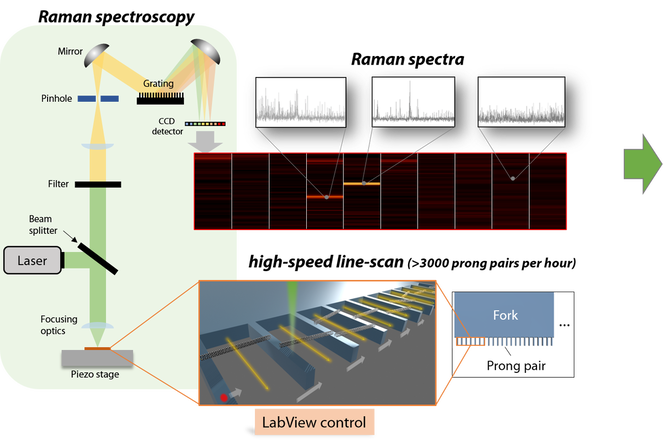
To image the SWNTs on the fork-like substrate, a confocal Raman imaging system with a high-speed camera, a fast piezo stage and a high-resolution stepper has been installed. We use a high-speed line-scan approach to determine the number, position as well as properties of the SWNTs. This approach takes only hundreds of milliseconds for each trench and achieves a final imaging speed of over 3000 trenches per hour. The full imaging on the fork-like substrate is automated and controlled via a LabView interface. Contact: Dr. Jian Zhang Involved research groups: Empa, Transport at Nanoscale Interfaces Laboratory Identification of carbon nanotubes using deep learning

We developed a high-throughput approach to rapidly identify suspended metallic (M-CNT) and semiconducting (S-CNT) carbon nanotubes by using high-speed Raman imaging and deep learning analysis. Even for Raman spectra with extremely low signal-to-noise ratios (SNR) of close to 1, we achieve a classification accuracy that exceeds 90%. Our approach can readily be extended to other types of nanomaterials and has the potential to be integrated into a production line to monitor the quality and properties of nanomaterials during fabrication. Contact: Prof. Dr. Martin Jaggi Involved research groups: Empa, Transport at Nanoscale Interfaces Laboratory; EPFL, Machine Learning and Optimization Laboratory NanoAssembler: Fully Automated Carbon Nanotube Integration
The assembly of ultraclean carbon nanotube devices has been a tedious and slow process for a long time. During this project, our team developed a machine, which has speeded up and simplified this task significantly. It transfers fully automatically carbon nanotubes from a growth into a device chip, one by one . With a rate of over 300 transfers/hour it already exceeds the previously reported rates by a factor of 300, enabling wafer level production. In the video, a microscopic footage of a transfer motion is shown alongside the machine. Contact: Dr. Natanael Lanz Involved research groups: ETH Zurich, Institute of Machine Tools and Manufacturing; Empa, Transport at Nanoscale Interfaces Laboratory PUBLICATIONS
2020
Pagliardini, M., M. Jaggi, F. Fleuret and S. P. Karimireddy (2022). "Agree to Disagree: Diversity through Disagreement for Better Transferability." ICLR 2023: arXiv-2202.04414. Zhang, J., M. L. Perrin, L. Barba, J. Overbeck, S. Jung, B. Grassy, A. Agal, R. Muff, R. Brönnimann, M. Haluska, C. Roman, C. Hierold, M. Jaggi and M. Calame (2022). High-speed identification of suspended carbon nanotubes using Raman spectroscopy and deep learning. Microsystems & Nanoengineering 8(1): 19. 2021
Jung, S., R. Hauert, M. Haluska, C. Roman and C. Hierold (2021). Understanding and improving carbon nanotube-electrode contact in bottom-contacted nanotube gas sensors. Sensors and Actuators B: Chemical 331: 129406. 2020
Cordonnier, J.-B., A. Loukas and M. Jaggi (2020). "On the Relationship between Self-Attention and Convolutional Layers." ICLR 2020: arXiv-1911.03584. 2019
Franceschi, J.-Y., A. Dieuleveut and M. Jaggi (2019). Unsupervised Scalable Representation Learning for Multivariate Time Series. NeurIPS. TEAM AND PARTNERS
Project Consortium
Prof. Dr. Michel Calame
Transport at Nanoscale Interfaces Laboratory (TNI), Empa Dr. Cosmin Roman Micro and Nanosystems (MNS), ETH Zürich Prof. Dr. Martin Jaggi Machine Learning and Optimization Laboratory (MLO), EPFL Prof. Dr. Konrad Wegener Institute of Machine Tools and Manufacturing (IWF), ETH Zürich
Involved and Supporting Industry Partners
➜ Iminia Technologies SA ➜ IST AG ➜ Sensiron AG ➜ WITec GmbH Leading Principal Investigator
|
|
An initiative of the ETH Board
|
Participating Institutions of the ETH Domain
|